Do you have any questions?
|
Technical sales iselRobotik Andreas Möller
|
 |
|
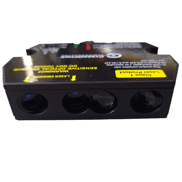
Wafer Mapping Sensor Cyberoptics
Wafer mapping sensors are used to detect the presence or absence and slotting errors (such as cross-slots) of semiconductor wafers in processing equipment.
They are typically mounted on robot arms or other wafer handling devices. EX-QS wafer mapping sensors are general-purpose wafer mapping sensors that excel at detecting even the most difficult to detect dark or coated wafers. EX-QS sensors can be used for notched or flatted wafers.
- light source: 2 x 850 mm diode lasers
- optimum detecting range: 38 mm (1.5")
- Maximum detecting range: 40 mm (1.6")
- Laser class 1
- PNP

